Products
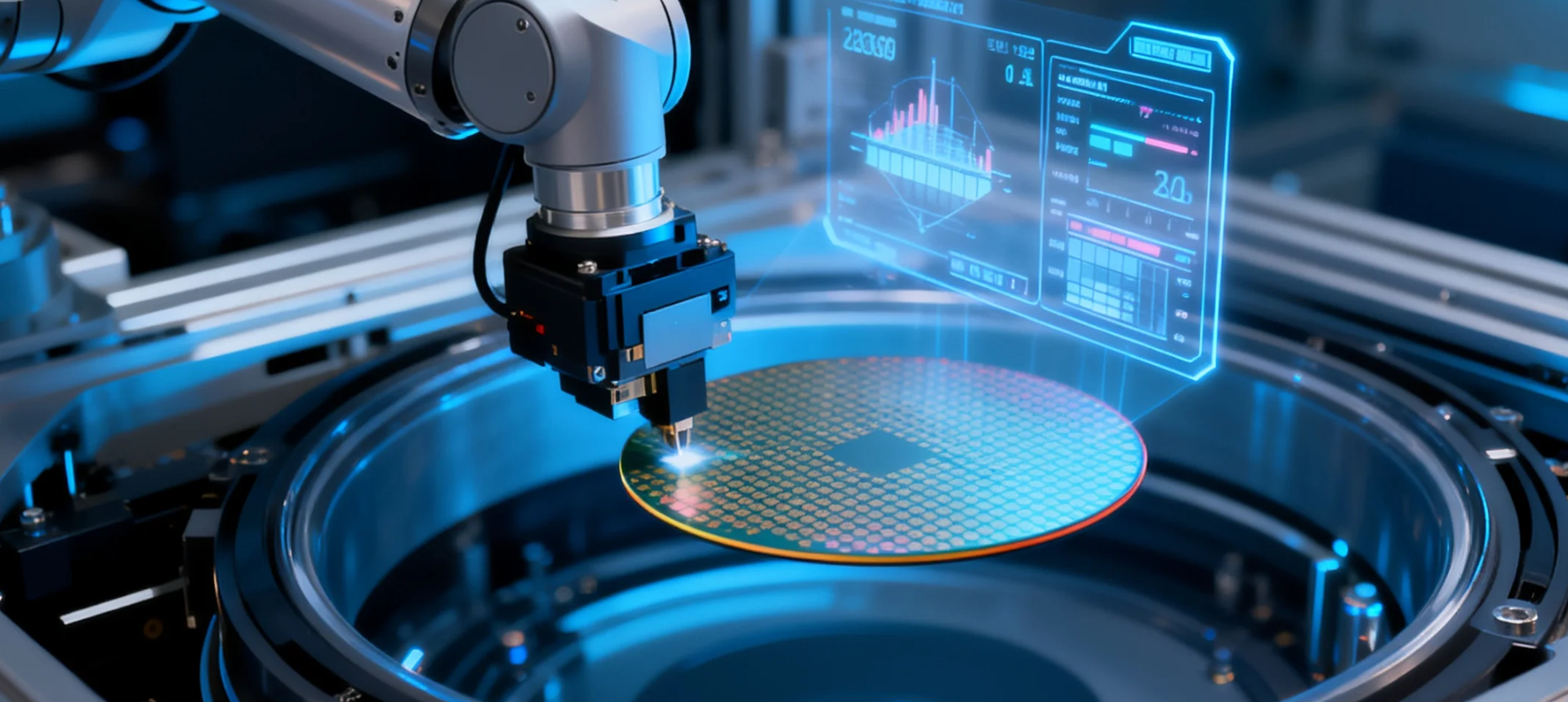
AI-Visual Inspection
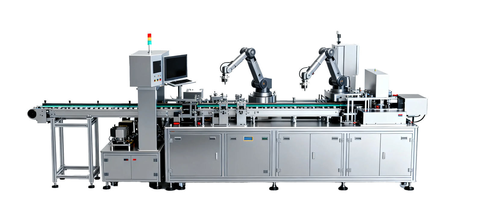
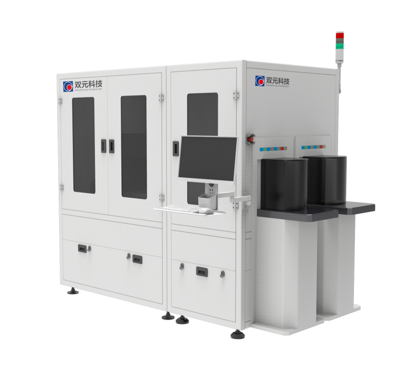
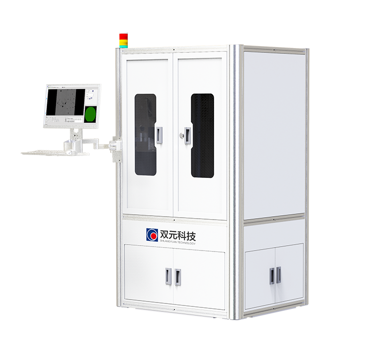
High-Speed Paper Defect Inline Inspection System Film Surface Defect Inline Inspection System Nonwoven Surface Defect Inline Inspection System Aluminum-Foil Surface & Pinhole Inline Inspection System Aluminum-Foil Carbon-Coating Surface Defect Inline Inspection System Copper-Foil Surface Defect Inline Inspection System Electrode Coating Width / Alignment / Burr / Surface Defect Inline Inspection System Cylindrical-Cell AI Visual Inspection System Vehicle Final-Assembly Vision Inspection SystemInformation Integration Control
Papermaking QCS Papermaking DCS Steam & Condensate System (SCS) Film Thickness Inline Measurement & Control System Film Coating-Weight Inline Measurement System Nonwoven Basis-Weight & Moisture Inline Measurement & Control Copper-Foil Basis-Weight / Thickness / Gloss Inline Inspection System Foil-Forming CD Basis-Weight Control System Aluminum-Foil Thickness / Gloss Inline Inspection System Aluminum-Foil Carbon-Layer Thickness Inline Measurement & Control Electrode Basis-Weight Inline Measurement & Closed-Loop Control Laser (High-Precision Spectral-Confocal) Thickness / Basis-Weight Dual-Probe All-in-One Electrode Winding Thickness Monitoring System PV Backsheet Thickness Measurement Wet-Laid Nonwoven DCS